
Description
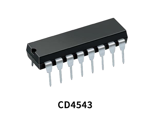
CD4543 Pinout
CD4543 Truth Table
It can be seen from the truth table that A, B, C, and D are four-digit BCD code input pins. And a, b, c, d, e, f, g are the position codes of the seven segments displayed by seven-segment characters.
When BI (Blanking) is 1 (high level), the output is no display state.
When BI is 1, LD is 0, the display will not change.
When BI is 1, LD is 1, the seven-segment code display output changes according to the BCD code input.
At this time, if the DCBA is a code input of 0-9, the output will display 0-9 respectively. If the DCBA is a code input of 10-15, the output will not display. Pin 9 (VDD) and Pin 8 (Vss) are power + and power ground.
CD4543 Advantages
CD4543B differs from the CD4056B in that it has a display blanking capability instead of a level-shifting function and requires only one power supply. When the CD4056B is used in the level shifting mode, two power supplies are required. When the CD4543B is used for LCD applications, a square wave must be applied to the PHASE input and the backplane of the LCD device. For LED applications a logic 1 is required at the PHASE input for common-cathode devices; a logic 0 is required for common-anode devices (see truth table).
The CD4543B is supplied in 16-lead dual-in-line plastic packages (E suffix), 16-lead small-outline packages (M, M96, MT, and NSR suffixes), and 16-lead thin shrink small-outline packages (PW and PWR suffixes).
CD4543 Features
Display blanking of all illegal input combinations
Latch storage of code
Capability of driving two low power TTL loads, two HTL loads, or one low power Schottky load over the full rated-temperature range
Pin-for-pin replacement for the CD4056B (with pin 7 tied to VSS)
Direct LED driving capability
100% tested for quiescent current at 20 V
Maximum input current of 1 µA at 18 V over full package-temperature range; 100 nA at 18 V and 25°C
Noise margin (full package-temperature range) =
1 V at VDD = 5 V
2 V at VDD = 10 V
2.5 V at VDD = 15 V
5-V, 10-V, and 15-V parametric ratings
Meets all requirements of JEDEC Tentative Standard No. 13B, “Standard Specifications for Description of ’B’ Series CMOS Devices”
Reviews
There are no reviews yet.